(China (Mainland))


Product Summary
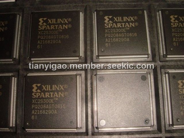
The XC2S300E-6PQ208I is a 1.8V Field-Programmable Gate Array. It offers densities ranging from 50,000 to 300,000 system gates. System performance is supported beyond 200 MHz. The XC2S300E-6PQ208I delivers more gates, I/Os, and features per dollar than other FPGAs by combining advanced process technology with a streamlined architecture based on the proven Virtex-E platform. Features include block RAM (to 64K bits), distributed RAM (to 98,304 bits), 19 selectable I/O standards, and four DLLs (Delay-Locked Loops). The XC2S300E-6PQ208I avoids the initial cost, lengthy development cycles, and inherent risk of conventional ASICs.
Parametrics
XC2S300E-6PQ208I absolute maximum ratings: (1)Supply voltage relative to GND:–0.5V to 2.0V; (2)Supply voltage relative to GND:–0.5V to 4.0V; (3)Input reference voltage:–0.5V to 4.0V; (4)Input voltage relative to GND:–0.5V to 4.0V; (5)Voltage applied to 3-state output:–0.5V to 4.0V; (6)Storage temperature (ambient):–65℃ to +150℃; (7)Junction temperature:+125℃.
Features
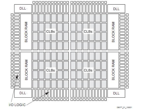
XC2S300E-6PQ208I features: (1)Densities as high as 6,912 logic cells with up to 300,000 system gates; (2)Streamlined features based on Virtex-E architecture; (3)Unlimited in-system reprogrammability; (4)Very low cost; (5)Fully 3.3V PCI compliant to 64 bits at 66 MHz and CardBus compliant; (6)Low-power segmented routing architecture; (7)Full readback ability for verification/observability; (8)Dedicated carry logic for high-speed arithmetic; (9)Efficient multiplier support; (10)Cascade chain for wide-input functions; (11)Abundant registers/latches with enable, set, reset; (12)Four dedicated DLLs for advanced clock control; (13)Four primary low-skew global clock distribution nets; (14)IEEE 1149.1 compatible boundary scan logic; (15)Low cost packages available in all densities; (16)Family footprint compatibility in common packages; (17)19 high-performance interface standards, including LVDS and LVPECL; (18)Up to 120 differential I/O pairs that can be input, output, or bidirectional; (19)Zero hold time simplifies system timing; (20)Fully automatic mapping, placement, and routing; (21)Integrated with design entry and verification tools.
Diagrams
 |
 XC2S100 |
Other |
|
Data Sheet |
Negotiable |
|
||||||
|
XC2S100-5FG256C |
|
IC FPGA 2.5V 600 CLB'S 256-FBGA |
Data Sheet |
|
|
||||||
|
XC2S100-5FG256I |
|
IC FPGA 2.5V I-TEMP 256-FBGA |
Data Sheet |
|
|
||||||
 |
XC2S100-5FG456C |
|
IC FPGA 2.5V 600 CLB'S 456-FBGA |
Data Sheet |
|
|
||||||
|
XC2S100-5FG456I |
|
IC FPGA 2.5V I-TEMP 456-FBGA |
Data Sheet |
Negotiable |
|
||||||
|
XC2S100-5FGG256C |
|
IC SPARTAN-II FPGA 100K 256-FBGA |
Data Sheet |
|
|
||||||