(China (Mainland))

Product Summary
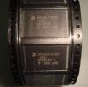
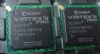
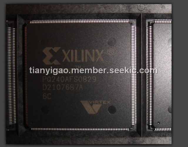
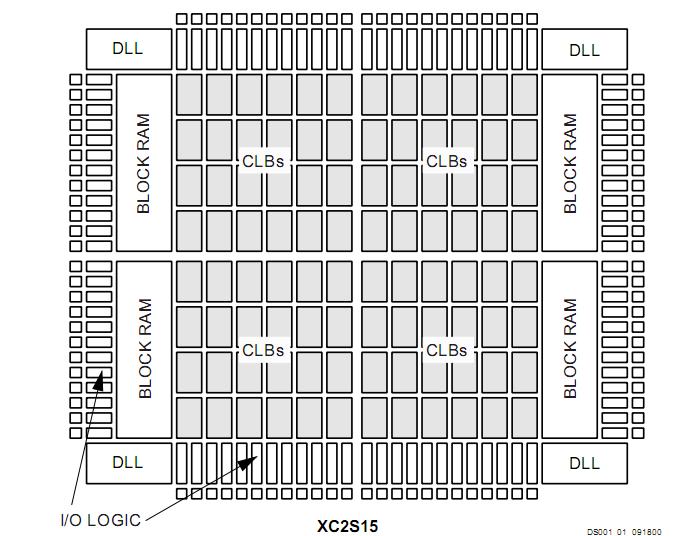
The XCV300E-6PQ240C is a FPGA. It has a regular, flexible, programmable architecture of Configurable Logic Blocks (CLBs), surrounded by a perimeter of programmable Input/Output Blocks (IOBs). The XCV300E-6PQ240C is customized by loading configuration data into internal static memory cells. Unlimited reprogramming cycles are possible with this approach. Stored values in these cells determine logic functions and interconnections implemented in the FPGA. The XCV300E-6PQ240C is typically used in high-volume applications where the versatility of a fast programmable solution adds benefits. The device is ideal for shortening product development cycles while offering a cost-effective solution for high volume production.
Parametrics
XCV300E-6PQ240C absolute maximum ratings: (1)Supply voltage relative to GND:–0.5V to 3.0V; (2)Supply voltage relative to GND:–0.5V to 4.0V; (3)Input reference voltage:–0.5V to 3.6V; (4)Input voltage relative to GND:5V tolerant I/O:–0.5V to 5.5V, No 5V tolerance:–0.5V to VCCO+0.5V; (5)Voltage applied to 3-state output:5V tolerant I/O:–0.5V to 5.5V, No 5V tolerance:–0.5V to VCCO +0.5V; (6)Storage temperature (ambient):–65℃ to +150℃; (7)Junction temperature:+125℃.
Features
XCV300E-6PQ240C features: (1)Densities as high as 5,292 logic cells with up to 200,000 system gates; (2)Streamlined features based on Virtex FPGA architecture; (3)Unlimited reprogrammability; (4)Very low cost; (5)Cost-effective 0.18 micron process; (6)Fully PCI compliant; (7)Low-power segmented routing architecture; (8)Full readback ability for verification/observability; (9)Dedicated carry logic for high-speed arithmetic; (10)Efficient multiplier support; (11)Cascade chain for wide-input functions; (12)Abundant registers/latches with enable, set, reset; (13)Four dedicated DLLs for advanced clock control; (14)Four primary low-skew global clock distribution nets; (15)IEEE 1149.1 compatible boundary scan logic; (16)Pb-free package options; (17)Low-cost packages available in all densities; (18)Family footprint compatibility in common packages; (19)16 high-performance interface standards; (20)Hot swap Compact PCI friendly; (21)Zero hold time simplifies system timing; (22)Core logic powered at 2.5V and I/Os powered at 1.5V, 2.5V, or 3.3V; (23)Fully supported by powerful Xilinx ISE development system:Fully automatic mapping, placement, and routing.
Diagrams
 |
 XCV300 |
Other |
|
Data Sheet |
Negotiable |
|
||||
|
XCV300-4BG352C |
|
IC FPGA 2.5V C-TEMP 352-MBGA |
Data Sheet |
Negotiable |
|
||||
|
XCV300-4BG352I |
|
IC FPGA 2.5V I-TEMP 352-MBGA |
Data Sheet |
Negotiable |
|
||||
|
XCV300-4BG432C |
|
IC FPGA 2.5V C-TEMP 432-MBGA |
Data Sheet |
Negotiable |
|
||||
|
XCV300-4BG432I |
|
IC FPGA 2.5V I-TEMP 432-MBGA |
Data Sheet |
Negotiable |
|
||||
|
XCV300-4FG456C |
|
IC FPGA 2.5V C-TEMP 456-FBGA |
Data Sheet |
Negotiable |
|
||||